What do you do when you need to validate the footprint of a SMD for an in progress product PCB ?
You run a test, and build another PCB of course… and by that I mean, you start another project… Might as well try to make it useful for future prototyping!
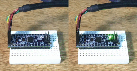
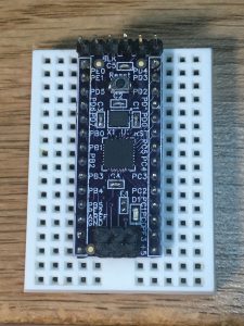
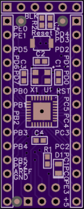
So here is the first pass (VT-X101-1) result of my effort to validate the footprint for an ATmega328PB-MU AVR CPU 32 pin QFN package, in a breadboard friendly form factor. Narrow enough to give you some room on the breadboard for components and wires, and only as long as needed to get all the pins out.
A sibling to the very popular ATMega328P, the ATMega328PB sports an additional UART and an additional I2C controller, something I’ve been wishing for and perfect for some of my future needs.


Once I assembled the board, I supplied power to the board with the FTDI cable, and programed it using my AVR JTAGICE3.
I proceeded to load it with the traditional hello world blinky program, but the blink interval was WAY longer than it was supposed to be.
Experience has taught me that this is usually the result of incorrect fuse settings, that CKDIV8 is still programmed or something. After multiple reviews of the fuse settings, and attempts to get the frequency correctly set, I came to the conclusion that something was wrong with my crystal or layout. After doing a part lift and replace, (self doubt is a bitch) to try and find something wrong, and while reviewing the board layout in gerbv, it struck me that, when I placed the crystal loading caps and the bypass cap adjacent to the crystal, I had accidentally swapped one of the loading caps with an adjacent bypass cap. Call me silly, but I just don’t understand why a .1uF won’t work for a loading cap! A quick swap of the caps, and correct fuses settings, and voila, correct frequency operation. Sorted!
With that, I loaded a minor variant of the ADABootloader, from a few years back, for which I changed the LED pin. The current source is linked at the top of the Adafruit Bootloader page. My version of the source is on GitHub along with a few frequency variations of the hex files.
I loaded the bootloader with “avrdude -patmega328pb -cjtag3isp-Uflash:w:ADABoot_328PB_x.hex -Ulfuse:w:0xFF:m -Uhfuse:w:0xD8:m -Uefuse:w:0xF7:m –Ulock:w:0xCF:m” where x is 16, 18, or 20. The Lock bits should keep the bootloader from being overwritten.
Now I can load blinky via serial (FTDI cable) with”avrdude -patmega328pb -cstk500v1 -b57600 …”
Huzza! There you have it. Just that easy! (not.)
What did I learn ?
Well, a few things;
- As soon as I got the boards in the mail, I could tell that the QFN32 foot print was gonna work correctly. Much to my delight, it worked much better that I expected for hand assembly! I tried to mis-align the QFN during my last lift and replace attempt, of which there were two or three, to find pad problems, and I just couldn’t.
- ALWAYS, and I mean always, pay attention to where you load parts onto a board. Even if you know where they go. This is twice in as many weeks that in-attention to silly little passives, has bitten me in the p’tushka.
- I need to be a bit more confident about my work results effort.
- Oh yeah… pay attention to plane fills. They aren’t magic. ie. they can become disconnected depending on how your traces are routed!
So I fixed two things (second pass, VT-X101-2, shown below);
- Bottom side GND plane fill
- Added a #RESET pull-up that I didn’t think was necessary, to possibly help with the FTDI reset sequence (un-tested).

Info;